Understanding Comparators: From Basics to Double-Tail Design
A detailed walkthrough of comparator design techniques, culminating in an efficient double-tail architecture for high-performance analog-to-digital converters.
Introduction to Comparators
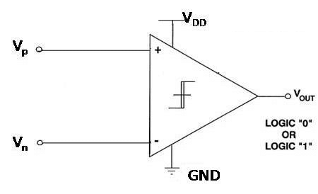
A comparator is a fundamental electronic component that serves as the backbone for many analog-to-digital conversion applications. As the name suggests, its primary function is to compare two voltage inputs and produce a digital output based on their relationship.
At its core, a comparator operates by evaluating two input voltages: when the voltage at the non-inverting input (V+) exceeds the voltage at the inverting input (V-), the output switches to a logical "1" (typically the supply voltage). Conversely, when V+ is less than V-, the output switches to a logical "0" (typically ground). This binary decision-making capability makes comparators very important in circuits that bridge the analog and digital domains.
Comparators in Analog-to-Digital Converters
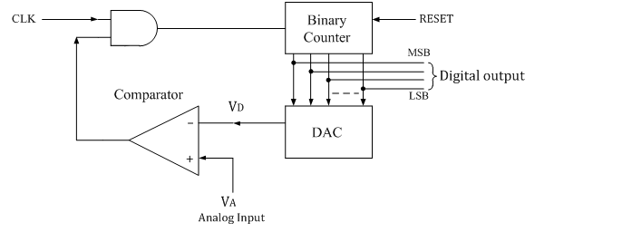
Analog-to-Digital Converters (ADCs) rely heavily on comparators to transform continuously varying analog signals into discrete digital values. In these applications, comparators act as decision elements that determine whether an input signal has crossed specific threshold levels.
When designing a comparator for ADC applications, several factors must be considered: speed and response time, input offset voltage, power consumption, noise immunity, and resolution requirements. The ideal comparator would have infinite gain, zero offset, and instantaneous response time—though in practical designs, this is impossible.
CMOS Inverter as a Simple Comparator
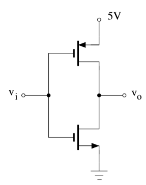
The simplest type of comparator is a CMOS inverter. It takes a single input Vin, and if Vin is greater than the trip point of the inverter, it will output a 0, otherwise 1. We can cascade another inverter after it to get the true logical value.
You might wonder about the reference voltage input—there isn't one in the traditional sense. The reference voltage is actually set by sizing the two transistors carefully. In a normal CMOS inverter, W/L of PMOS is roughly 2-3 times that of NMOS, due to the difference in carrier mobility (μn ≈ 2-3 × μp). This sizing helps achieve a switching threshold of VDD/2 when both transistors have similar threshold voltages.
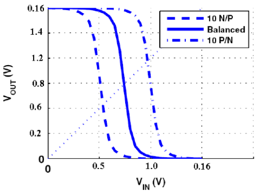
We can also set the trip point at whatever fraction of the supply voltage we want by changing the sizing. For example, if VDD is 5V and we want the trip point at 2.5V, then W_p is roughly 2 * W_n. If we want a trip point at 1 volt, then we'll make W_n much bigger. Conversely, for a higher trip point, we increase the size of W_p.
The CMOS inverter approach has a couple of advantages: it's incredibly simple with minimal design time needed, has less power draw, and takes up less area. Unfortunately, there are many drawbacks too. First and foremost, it's not very accurate due to process variations that affect the threshold voltage and size, resulting in inconsistent switching points and reduced precision in analog applications. The lack of gain also means that small input differences may not be properly amplified, leading to weak noise margins and increased susceptibility to interference. It's suitable only for extremely low-resolution applications.
Op-Amp as a Comparator
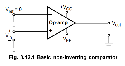
Departing from the CMOS inverter, the next step up is using an operational amplifier as a comparator. The open-loop output of an op-amp is equal to Vo = Ao(V+ - V-), meaning the difference between the signals gets multiplied by the open-loop gain. Usually, the open-loop gain of an op-amp is very large (often exceeding 10^5 or more), so the output should saturate to ground and VDD, giving us digital outputs.
When using an op-amp as a comparator, Vref would be connected to the inverting terminal, and Vin would be connected to the non-inverting terminal.
The advantages of using an op-amp include high sensitivity due to the extremely high open-loop gain, adjustable reference voltage by setting Vref, and improved noise immunity since the output is driven to the rails, making digital logic level transitions generally robust against small noise fluctuations.
However, there are drawbacks: slower response time as general-purpose op-amps are designed for linear amplification and may have slower slew rates compared to dedicated comparators, potential lack of rail-to-rail output in some cases requiring additional circuitry, and large input offset voltage since op-amps are optimized for linear operation.
The Double-Tail Comparator
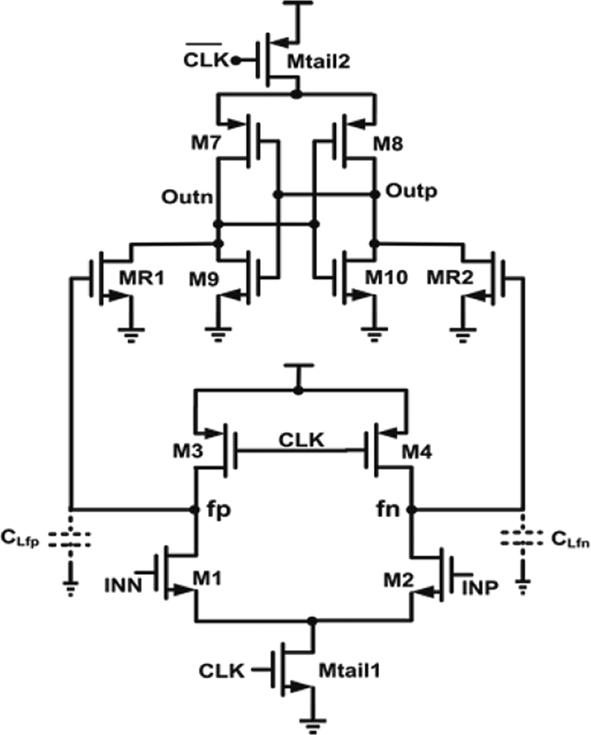
The double-tail comparator architecture is found at the heart of many data converters for good reason. It's a dynamic comparator design, meaning it does not require a constant bias current and operates based on clocked switching. Dynamic comparators are commonly used in power-sensitive applications because they only consume power during the evaluation phase, making them more efficient than static comparators.
There are three stages in this particular comparator design: preamplification, track, and S/R latch. To get good performance out of a comparator, we first want to amplify the difference between the signals before feeding it into the actual comparison stage. This increases the speed of the decision time and separates the input from the extremely high slew rate latch, which may introduce kickback noise into the signal or reference voltage.
The preamplification stage helps to reduce the input-referred offset and noise, improving the overall accuracy of the comparator.
The Preamplifier Stage
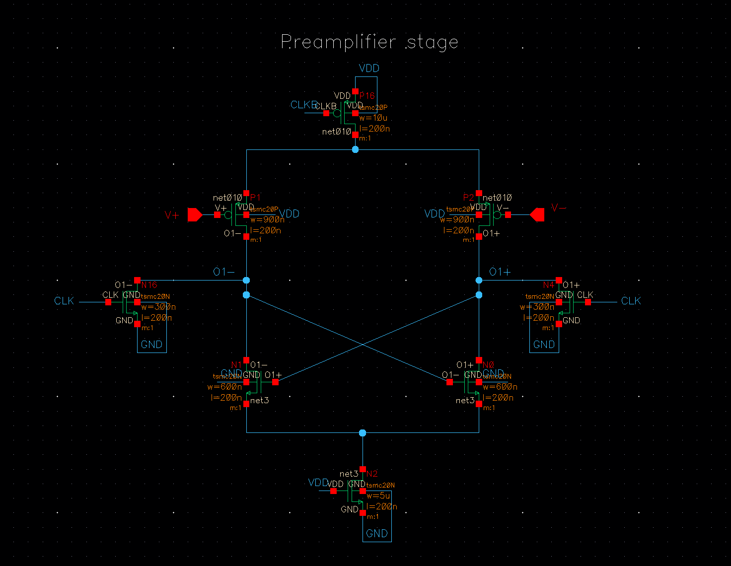
This cross-coupled pre-amplifier utilizes PMOS transistors as inputs with cross-coupled NMOS transistors forming a regenerative load, alongside NMOS tail current sources. The input pair is implemented with PMOS transistors to reduce the input-referred noise, as PMOS devices typically have lower 1/f noise compared to NMOS transistors.
This circuit operates in two distinct phases: reset and compare. During the reset phase when CLK is high, transistors N4 and N16 pull the outputs low, discharging node capacitances to prevent the circuit from becoming stuck in one state. When transitioning to the compare phase as CLK goes low, N4 and N16 turn off, allowing the cross-coupled NMOS pair to begin its regeneration process with effectively infinite gain.
This positive feedback mechanism amplifies small current imbalances through the PMOS inputs, creating voltage differences that are further amplified by the cross-coupled NMOS pair. The feedback continues until outputs reach the supply rails.
Regarding current sources, the PMOS current source at the top has twice the width of the NMOS tail current source. Testing reveals that clocking the top PMOS current source improves performance while clocking the bottom NMOS current source degrades it. These current sources can operate either in static mode (always on) or dynamic mode (clocked), with clocking both reducing power consumption.
The Latch Stage
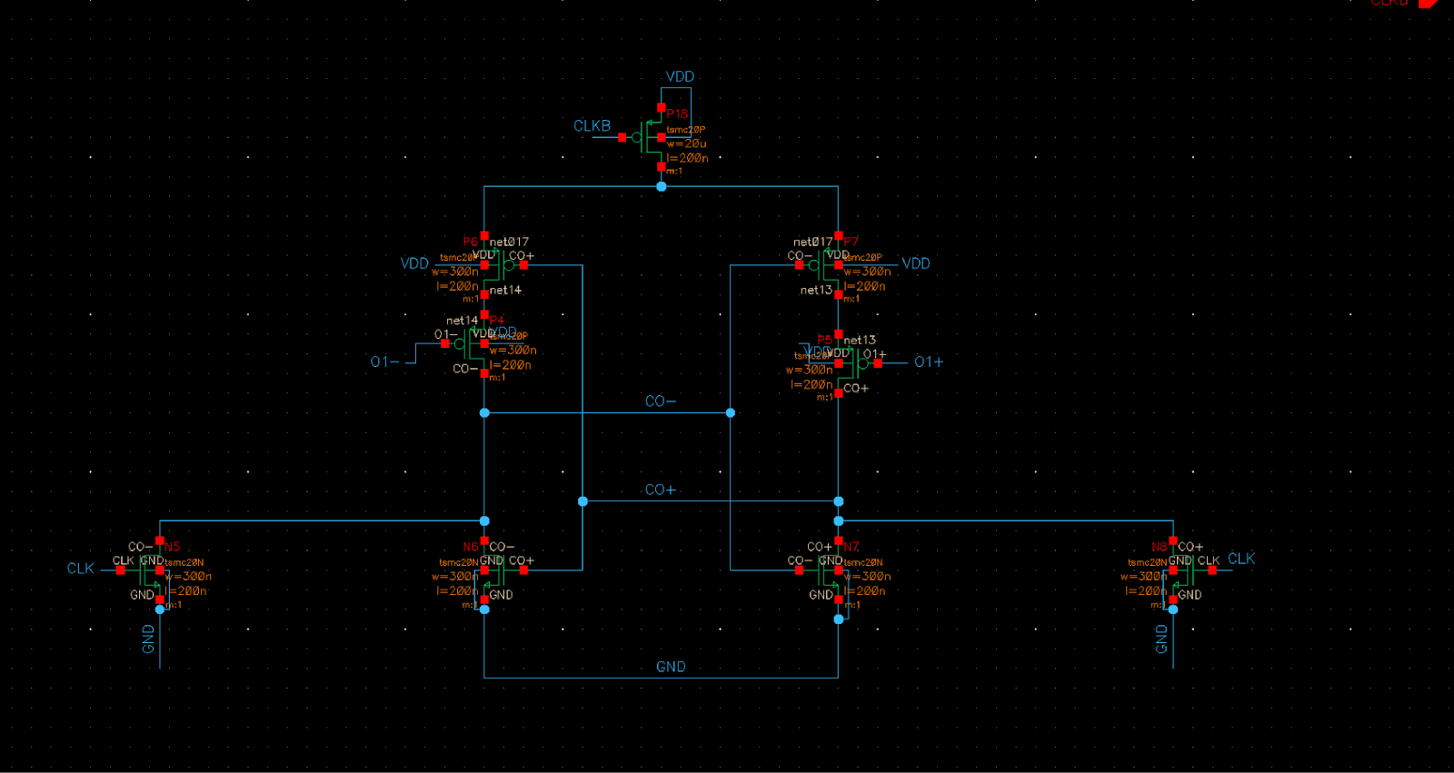
The output from the preamplifier stage (O1+, O1-) goes into the latch stage. The heart of the latch stage is in the back-to-back inverter pair.
When CLK is high, two transistors, N8 and N7, pull down the output nodes to ground during the reset phase. When the clock is low, the previous stage's output is applied to the transistors across the inverters, which begin to pull current. The positive feedback of the inverters dominates and again pulls the outputs to the rails at a large rate.
Reset and Regeneration Phases
During the Reset Phase (CLK High), transistors N5 and N8 act as reset switches, shorting both output nodes (Out+ and Out-) to ground, ensuring a well-defined initial state (Out+ = Out- ≈ 0V) before comparison begins.
As the clock transitions low in the Metastability Phase, N5 and N8 turn off, isolating the outputs. The preamplifier's small differential voltage (ΔV) introduces an imbalance in the cross-coupled inverters (P6, P7, N6, N7), where ΔV causes a slight current imbalance in the input MOSFET pair, leading to increased conduction in one branch.
Finally, in the Regeneration Phase, positive feedback rapidly drives the decision. If Out+ begins to rise, N6 strengthens conduction, pulling Out- lower, which further enhances P7's drive. The regeneration time constant is approximately τ = CL/gm, where CL is the load capacitance at the output nodes and gm is the transconductance of the regenerative pair. With a loop gain greater than unity, the voltage difference grows exponentially until the outputs reach the rails.
Performance Analysis
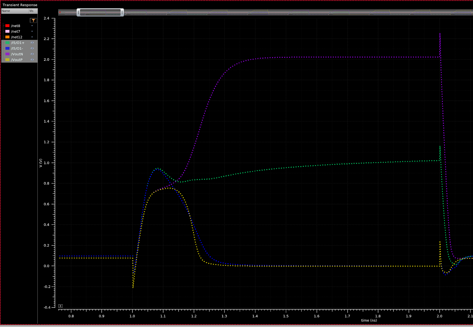
In the transient response, you can see the preamplifier stage labeled as o1+ and o1-, providing gain for the second stage to make a decision quicker, rising to VDD/2 in less than 200 ps.
If we were to connect the inputs only to the second stage, it takes 75% more time, needing more than 350ps to reach VDD/2.
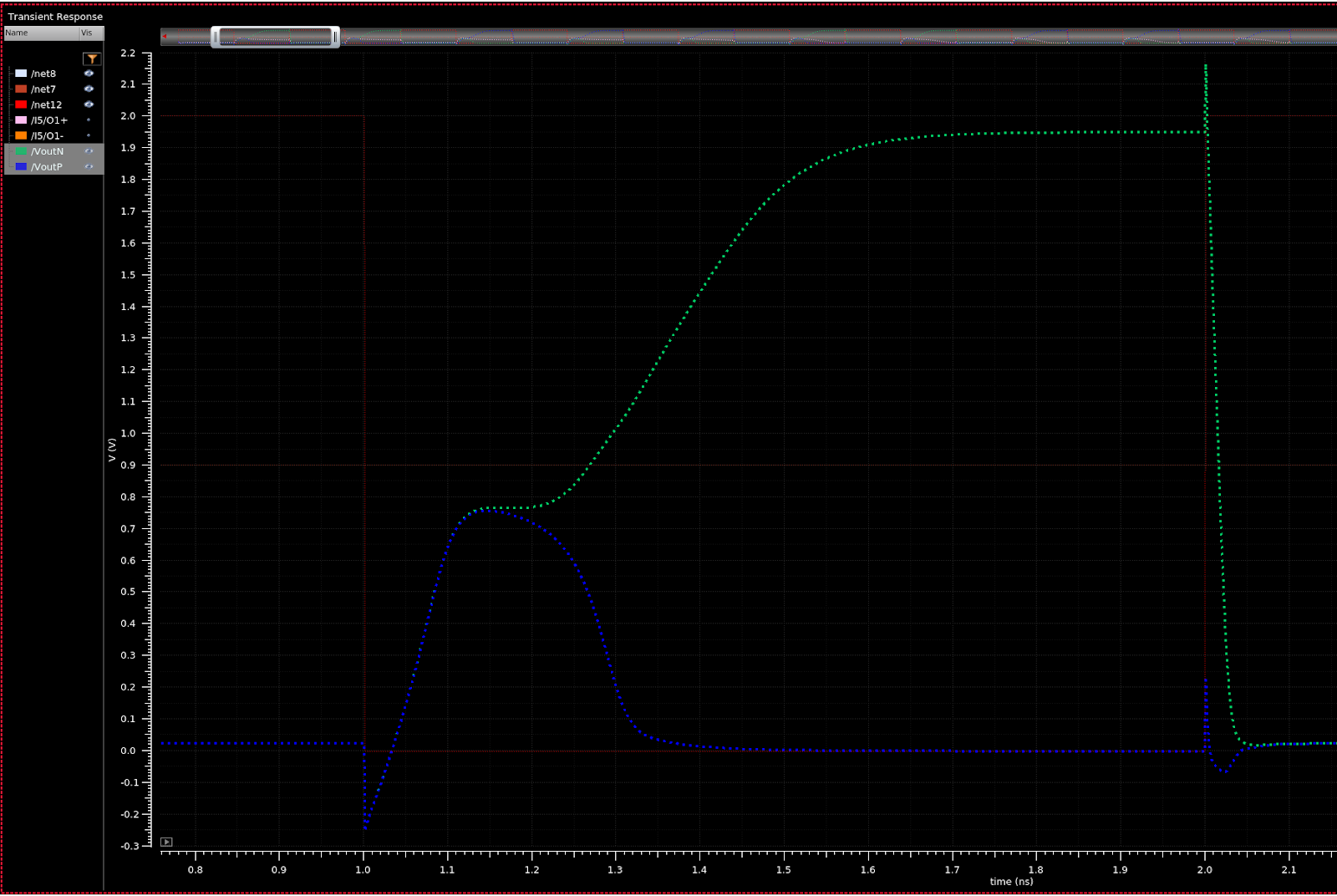
(almost) Final Design
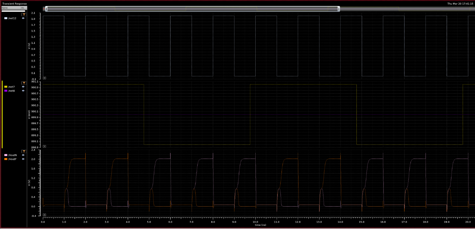
One issue with the design so far is that on the reset phase, we're not holding our value—it goes to 0. This is fixed with a set-reset latch: two cross-coupled NAND gates along with buffer inverters complete the design.
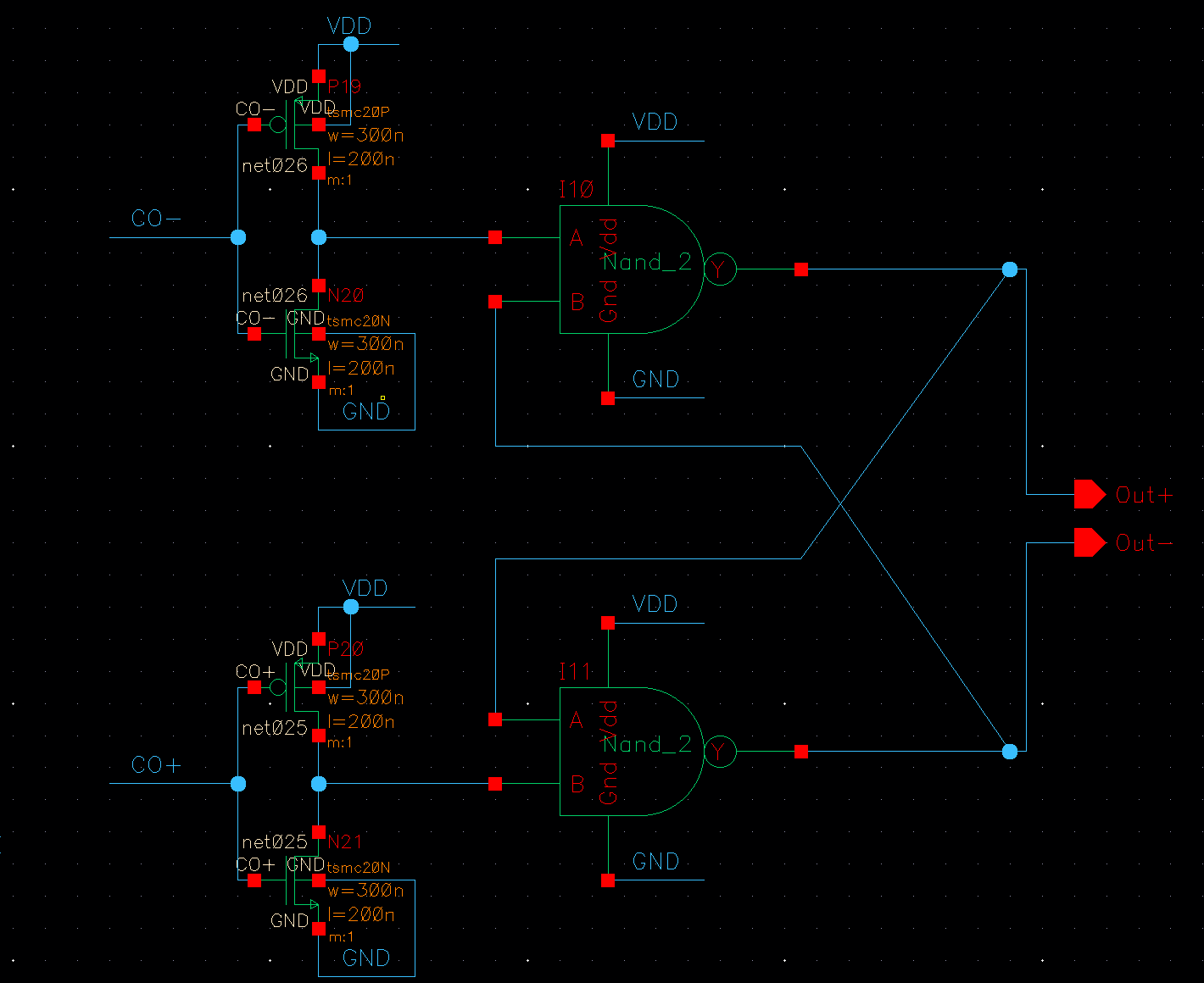
Final Design
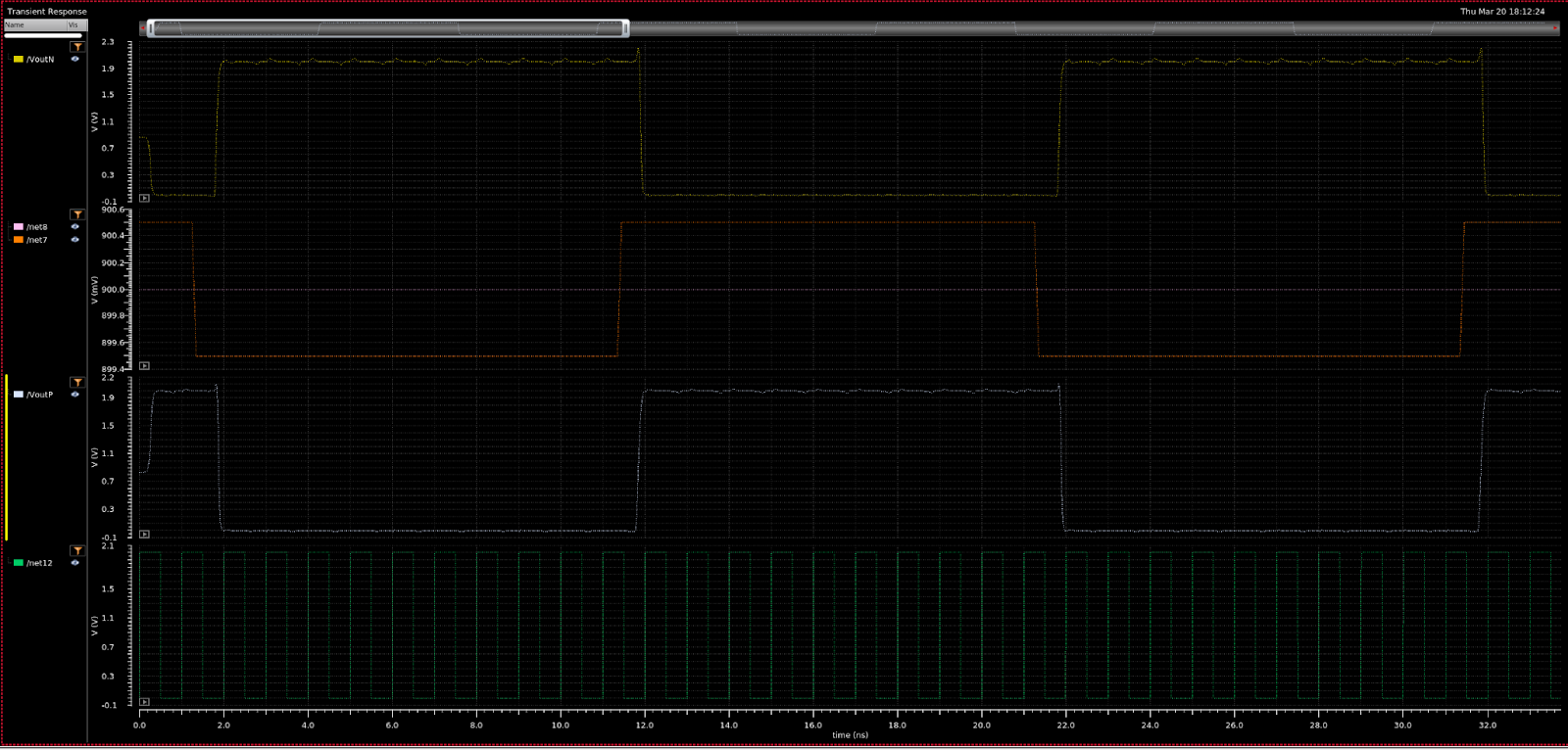
The final comparator has a common-mode voltage range of 0.6V to 1.4V, a delay of approximately 250ps, and can easily discern a 500µV input differential. Of course, these results come from ideal simulations, and real-world performance will have additional considerations.